Synth DIY: Stompbox Mixer
Recently I wanted to use two different effect pedals in parallel, but didn’t have anything handy that would easily allow me to split and then re-combine the signals. So I designed and built one! It’s a very simple device consisting of a passive multiple and a 3-into-1 audio mixer with input level pots and a single output.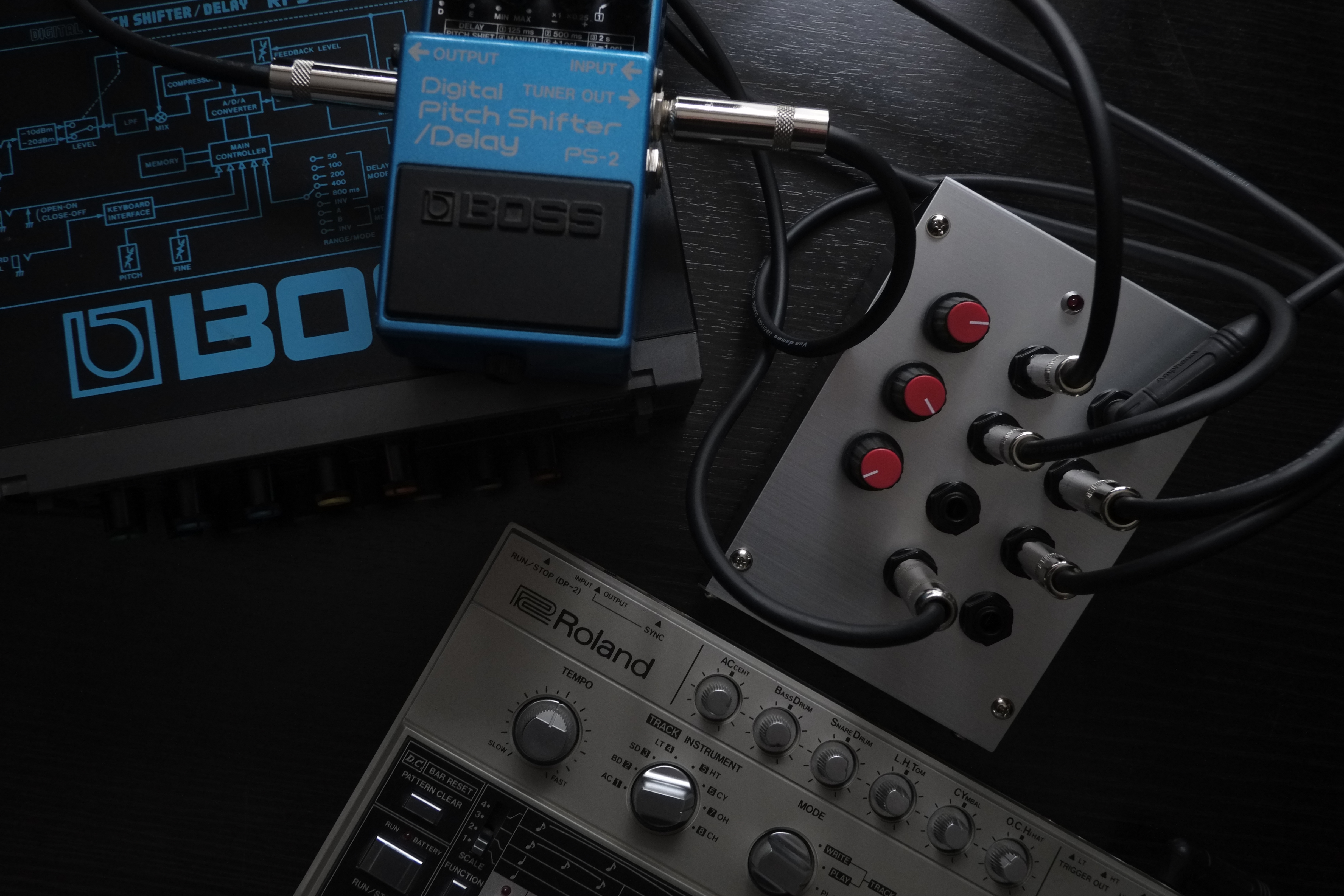
The mixer circuit uses a single transistor and runs from 9V DC, so you can power it from the same supply you use for your pedals. It draws only a few milliamps. The multiple is entirely optional – it’s purely passive and is just 4 jacks tied together, but it’s a useful addition and you could fit both this and the mixer into the same enclosure.
The Circuit
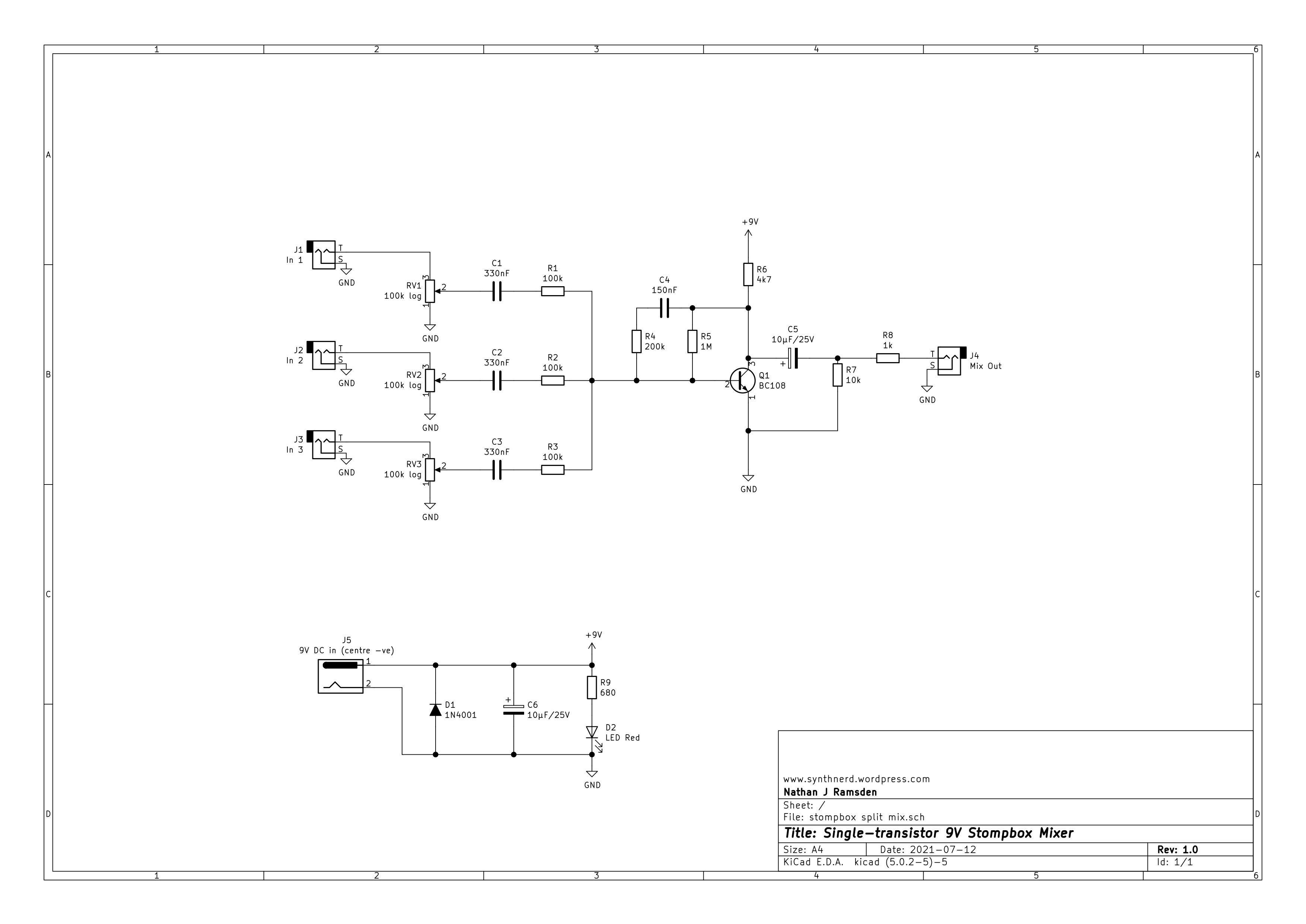 Here’s the schematic. It can also be downloaded as a PDF here.
How it Works
This is a very simple single-transistor design that uses a generic NPN device. The circuit is a ‘common emitter’ type (a basic description can be found here). Signals are presented to the base, and the output is taken from the collector. In order for the output to be able to swing up and down (audio signals are AC, don’t forget), the collector needs to sit somewhere a little above half way up the supply when nothing is happening. Given that we’re running this from 9V, it’s only really suited to relatively low audio signals, but we still have enough headroom for a small number of mixed inputs. I had no trouble mixing three audio test signals.
I won’t go into much detail about all aspects of the design process here, but the core is the transistor Q1, the resistor R6 from collector to 9V, and the resistor R5 from base to collector. The gain (Hfe) of Q1 together with these other values sets the collector voltage around which point the signals are mixed. The first job is to pick a transistor.
Transistor Selection
A simple way to choose a transistor is to build the test circuit shown here, using just Q1, R5, and R6. Connect power and measure the voltage at the collector. The aim is to get a voltage here a little over half supply, but not too much higher. Something in the region of 5V is fine. I picked a BC108 with Hfe of around 220, which was my starting point for the other component values in the circuit. The 2N3904 is also a good choice, and easy to find. Hfe is not a precise value for any device but a ballpark of 200 will suit nicely.
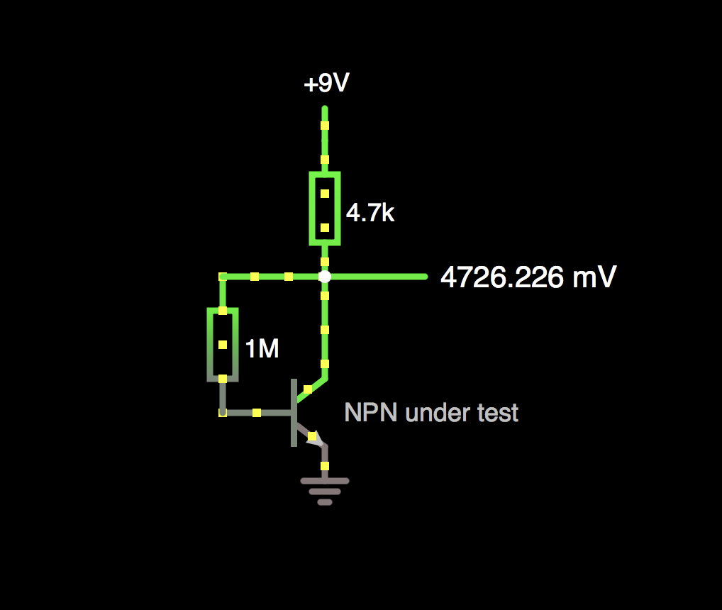
If you find your transistors all giving collector voltages nearer to 4.5V or even lower, and sourcing alternative devices is not an option, try decreasing the 4k7 resistor value – for example, if your Q1 Hfe is nearer 300, a 3k3 resistor will suit better.
I should stress here that this design is absolutely a compromise for the sake of simplicity. ‘Close enough’ is fine. The risks are lower headroom and some distortion.
The Rest of the Mixer Circuit
The inputs are brought in via potentiometers and decoupled using small capacitors. Three input resistors mix the signals into the transistor base. Note that the capacitor and resistor in series on each input acts as a low-cut filter to reduce sub-audio content.
In parallel with the 1M resistor discussed before, we add another resistor and capacitor across the NPN’s base/collector (R4 & C4). This does several things, not the least of which is to set the gain of the inputs. The 200k resistor, in tandem with the 100k values at the input, would suggest a gain of 2 (200k/100k = 2) but the real value is somewhat lower. In practice, with these values I found unity gain around 80% of the way around the input level pots, so there’s a little bit of boost available to help balance levels if you need it. The pots, by the way, should be log (or audio) taper.
Finally, the output is decoupled so that the signal has no DC offset and moves around 0V.
Powering the Circuit
I used a standard 9V DC barrel jack of the kind seen on many effect pedals – in this case the positive tends to be on the outer sleeve, and ground on the centre pin, Boss-style. A diode across the input protects against reverse connection, the capacitor helps smooth the incoming supply, and a resistor/LED draws a few milliamps to indicate ‘power on’.
The Passive Multiple
This is simply four jack sockets with their ground/sleeve connectors tied together and their tip connectors tied together. Please note, they are intended to split one signal several ways, not to combine signals.
*
… And Finally
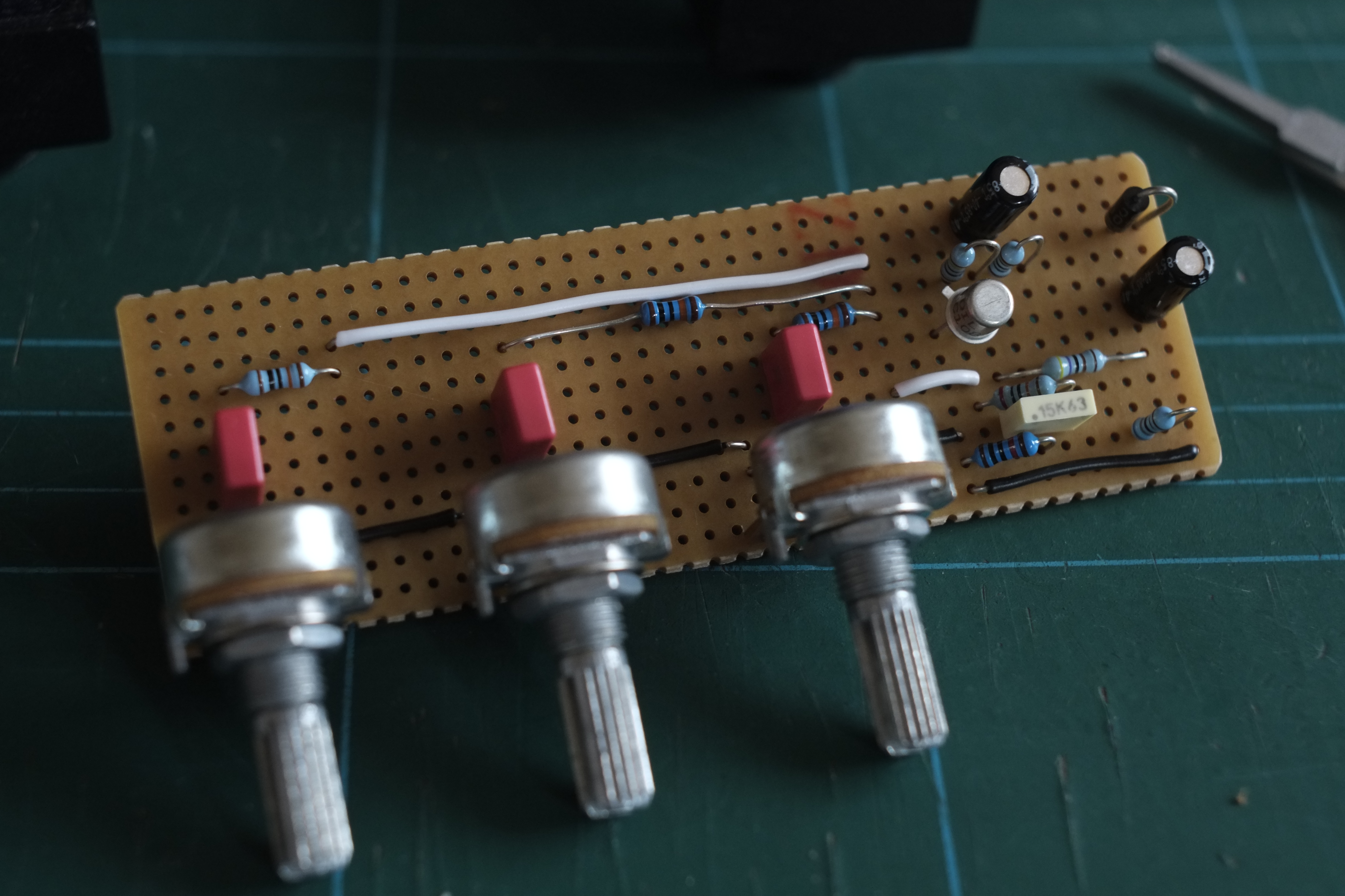
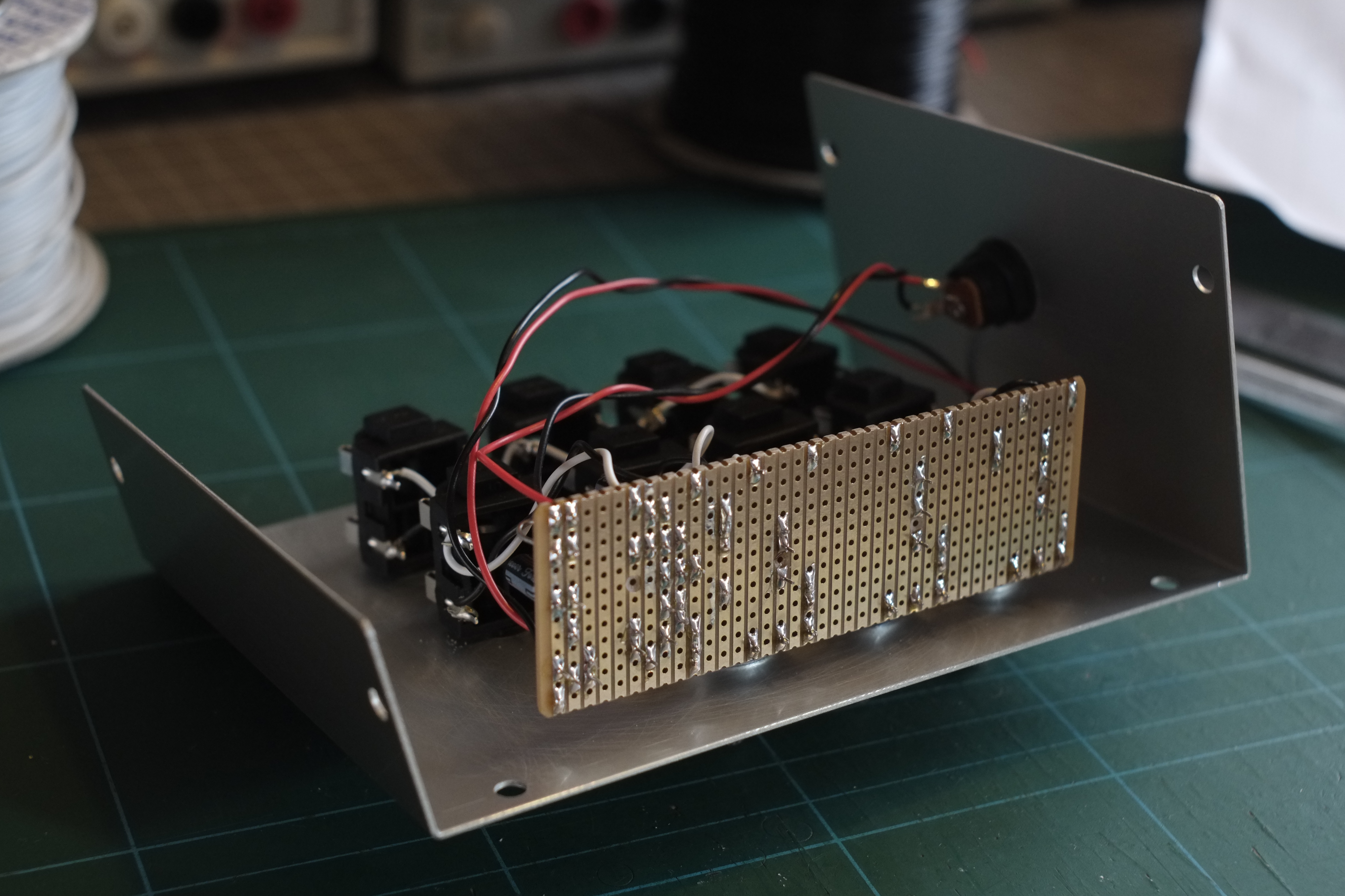
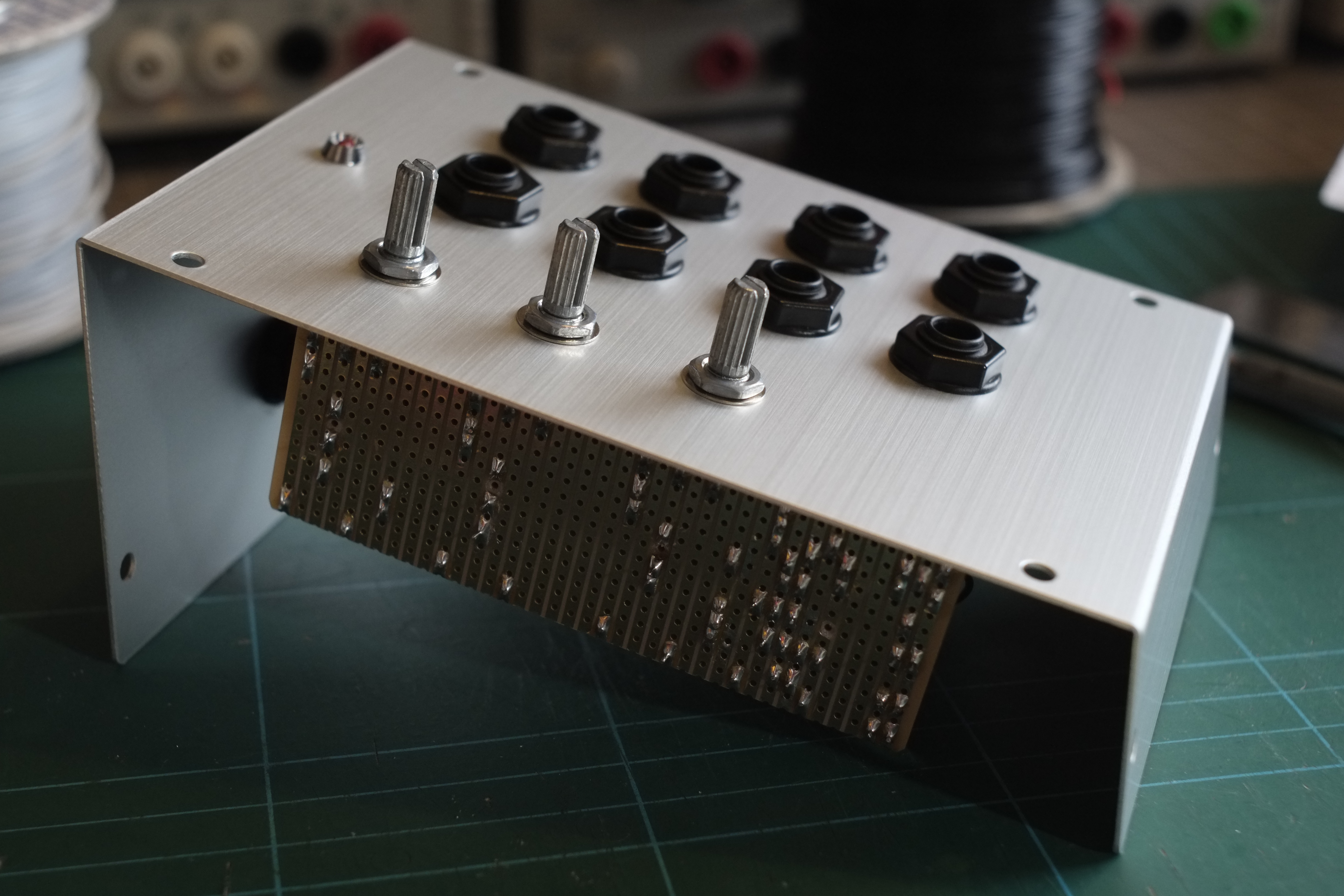
Here are some photos of the build. You can see there’s lots of room in that enclosure, but I wanted something that was stable on the desk with a few cables hooked in. It’s possible to make the final unit quite small as the circuit itself takes up very little room. Designing a layout is your only challenge. Of course you can use any kind of box, sockets, and knobs that you like. I hope you find this useful!

*
Synth DIY: a White Noise generator (part 2 of 2)
In Part 1 I outlined how to make a very simple discrete white noise generator. In Part 2 I’m going to expand that into something a little more interesting.
ADDING FILTERS
To colour the noise, simple passive filtering is sufficient. Originally I was going to put a switch here with a couple of different RC networks in place for basic high- and low-pass, but instead opted for a potentiometer to fade between them. The filter circuit below is inspired by part of the classic EMS VCS3 synthesizer, though is not identical. The pot sweeps from high pass at one end, through to low pass at the other, with a balance in the middle.

Schematic diagram of the white noise colouration filter
R4/C4/R5 and R6/C5 form low- and high-pass passive filters respectively. The pot pans between them by proportionally grounding one, or the other, or somewhere in between. The two networks have the same cutoff frequency, and that remains the same as you sweep the pot. It’s really just a balance control, between high and low frequency content.
OUTPUT BUFFER
Now we just add a volume control and one more stage of amplification to buffer the output. The overall output from the whole circuit, with these components, is about 5v p-p maximum. This varies as you sweep the filter. Feel free to play with the gain – line level audio will hover around 1v p-p, modular signals nearer 10v p-p.
You can download the full schematic as a PDF here.
Please Note: the schematic below includes corrected R and C numbering in the first stage. The schematic posted in Part 1 accidentally starts the numbering at 2 instead of 1. The component placement and values, however, should be correct throughout.

Discrete white noise generator schematic
CAN I USE A DIFFERENT VOLTAGE SUPPLY, eg. 12v or 15v?
The short answer is ‘yes’.
A single-sided DC supply is fine for the transistor circuits here, and 9v or more is sufficient to allow breakdown noise generation. If you use a dual supply, opamp stages would make for an efficient circuit with very easily controlled gain.
HOW DO I SELECT A TRANSISTOR?
Pick out any NPN you have at hand, connect its base to 0v and its emitter through a resistor to your positive supply. Leave the collector free. Power up and use a scope to monitor the noise at the emitter. Choose a resistor between 100k and 1M. Lower values give greater noise level, to a point. Too high resistance, and you won’t see a suitable noise source. The results listed in Part 1 for different devices were based solely on some quick practical tests, and are to be taken as a guide only.
You should be able to use pretty much any common general-purpose NPN in this manner, though don’t forget to pay attention to the pin arrangement as this varies across different devices.
*
Here’s a photo of the circuit in development on a breadboard. The scope shows the white noise output, the meter shows current consumption. Note the 9v PP3 battery providing power.

Photo of the white noise circuit during testing
Finally, here’s a couple of photos of the finished device, housed in a stompbox-sized enclosure, and with an LED added to show power on. The audio output is a 1/4″ mono jack, and the power input is a 3.5mm minijack. Not the most common style for 9v, but they do crop up, on old DOD pedals for example, and some EHX. It’s just what I had lying around.
The second photo of the pair shows the interior. You can see how the circuit fits easily enough into a small enclosure. The eagle-eyed reader may notice a component difference or two – that’s because the black box is a version I made some time ago, and I decided to recreate and update the design for this blog.
Enjoy!

Photo of the finished white noise box

Photo of the finished white noise box – interior
*
Synth DIY: a White Noise generator (part 1 of 2)
WHAT IS WHITE NOISE?
We’ve all heard white noise in synth patches – it sounds like the wind, adds breath to a pad, rattle to a snare. It’s also a useful source of randomness for modulation, either directly or via a sample and hold circuit.
Technically ‘white’ noise comprises all frequencies at all amplitudes. Despite this sounding complicated, we can generate white noise very simply. It happens naturally in transistors and all we have to do is amplify it.
Once we have our white noise, we can filter it. Different colours represent different frequency content. Many synthesizers only provide white noise, but some also offer pink, which has the high frequencies rolled off. Occasionally you’ll see noise labelled as blue, red, or brown.
METHOD
I decided to make this circuit using discrete components only – no ICs for once! You could use opamps instead for the amplifier stages, but the transistor circuit is compact and runs from a single supply, in this case 9 volts. Battery power is more than adequate.
BASIC WHITE NOISE GENERATOR
Please Note: the R and C numbering in this schematic accidentally begin at 2 rather than 1. This does not affect placement, values, or operation. These identification markers are corrected on the full schematic in Part 2.
Also note the pin arrangement for Q1 will vary depending on your choice of transistor.

Basic discrete transistor white noise generator schematic
HOW IT WORKS
The noise itself comes from the first transistor, Q1. In most circuits, the voltage at the base of an NPN would be higher than that at the emitter, allowing current to flow between the collector and the emitter (transistor basics here if you need them, there’s no shortage of guides on the internet). However, for noise purposes we reverse that – we hold the emitter higher than the base. We also leave the collector unconnected. If the reverse voltage applied is sufficient, it produces noise that we can amplify and use.
Here I’m using a BC182L. This component will require some experiment on your part. Every transistor has a different breakdown voltage (ie., the reverse base-emitter voltage that produces the noise), and every transistor will give different noise quality. I had good results with the BC182L, but I recommend trying whatever NPN devices you have at hand. If you have an oscilloscope, testing each transistor along with just resistor R2 (here I’m using a 1M resistor) is enough to compare a few examples. My selected BC182L with 1M on 9V gave noise levels up to 100mV peak-to-peak. The output was measured at the emitter.
The following image shows a sample from my Rigol 1054z oscilloscope. Horizontal divisions are 1ms, vertical divisions are 20mV. The bright band is the momentary snapshot, the dark band behind it is the signal smoothed out over time. You can see the signal is around 100mV from its highest to lowest point. This is pretty much the strongest result I got from any of my transistor stock.

Oscilloscope display of breakdown noise in a BC182L transistor
I also tried several other silicon NPN transistors – nothing special, just what I had handy. In order to get something in the region of 100mV p-p I had to change the resistor value for each of them. Here’s a quick list of my results:
2N3904 — 200k
These values are a guide only. You should adjust up or down as required – lower value to get a higher output. Something between 100k and 1M should give you useable noise from a broad range of transistors, so don’t worry if what you have isn’t listed here.
BUFFERING THE NOISE
The rest of the circuit around the second transistor Q2 is an amplifier. I won’t describe here how this works (feel free to research common emitter amplifiers), but with these parts the output was around 2V p-p. That should be loud enough for audio testing if you don’t have a scope. You could substitute an opamp stage here, which I won’t detail. Consider it homework ;).
Note the 10pF capacitor. This isn’t essential. In fact, the noise has a higher peak-to-peak level without it (see images below) but it will sound different. This small value capacitor rolls off the harsher top end frequencies, making the basic ‘white noise’ smoother. Adjust, or omit, to your taste.
I recommend prototyping this circuit hooked up to something you can listen with, as well as see the signal on a screen. The component values are not set in stone, and it’s worth experimenting.

White Noise figure with and without 10pF capacitor in feedback of transistor buffer stage
Finally for this stage we can add a capacitor on the output. This will decouple the output from any DC bias when we hook it to something else. You can see the DC bias in effect on the next image. Consider that we are using a single-sided 9V DC supply. The noise has to happen between two positive voltages. Audio signals should be centred around 0V. Any difference between 0V and the centre of the audio signal is the DC offset, and this can cause various problems such as distortion or even speaker damage. The DC offset in the image below is around 4.5V (the dotted horizontal line at the centre of the grid is 0V, the major divisions are 2V).

White Noise output from first stage buffer showing DC offset
The next image shows the same noise signal taken from after the capacitor but measured as an AC signal to remove the offset. See how it is bipolar around the centre point.

White Noise output from first stage buffer with DC offset removed
This is enough for a standalone white noise source, and if you choose your components well the output should be enough for audio. You may wish for more gain if you’re using this with a Eurorack modular or similar. Modular synth levels are around 10V p-p, and we’re not going to reach that with a 9V supply. Feel free to experiment with a 12V supply though. If you want to get a more substantial output, you can use a bipolar supply and an opamp gain stage instead of the second transistor. Alternatively, we’ll be adding an output stage later anyway.
Synth DIY: the LFO (an overview)

Some synth LFOs as they appear on the panel
What is an LFO?
LFO stands for Low Frequency Oscillator. It’s a general purpose modulation source that outputs a slowly cycling waveform. They are commonly used for effects such as vibrato, tremolo, PWM, and filter sweeps.
An LFO’s frequency is usually sub-audio, but in practice many LFOs venture into the low audio range (above 20Hz) or even higher. At the slow end, cycle time is a few seconds, sometimes a lot more – there’s no standard range for an LFO. Sometimes they’re just called ‘modulation oscillator’, which I guess is more accurate.
The output of an LFO will often be a sine or triangle wave, as they give good results for most purposes, but other waveforms are also common – square waves, ramps, and a ‘random’ or ‘sample and hold’ output are also popular (these are good for the ‘burbling’ effect often associated with synth sounds). Technically, a sample and hold circuit is another device, so I won’t cover that here.
Many older synths come with just one LFO, which means all your basic cyclic modulations (as opposed to one-shot modulations like envelopes, or stepped modulations like sequences) have to come from the same source. It would be better to have at least two LFOs, so that pitch modulation and PWM, for example, could use different waveforms at different speeds.
Happily, many new synths have multiple LFOs, and luckily for DIYers, making an LFO is a simple job. The parts are cheap and plentiful, the basic circuit is compact and easy to build, and one or two extra LFOs can enliven a basic synth patch considerably.
There are several ways to make such a circuit but I’ll limit myself here to two basic methods:
- the Relaxation LFO
- the Integration LFO
I’ll be adding links to designs on this page as I write up a few details, so bear with me!
Synth DIY: the Relaxation LFO
This circuit gets is name from the way it charges, then discharges, a capacitor. Think of it like breathing: inhale, exhale. The charge on the capacitor is the rhythm of the breath.

Relaxation LFO

Relaxation LFO simulation
Watch this in action here: Relaxation LFO simulator
Download a PDF of the schematic here: Relaxation LFO schematic
This example uses two op-amp stages, run from dual supply rails. Let’s consider just the first op-amp for now.
It has something in common with a comparator – the output will flip high or low depending on which input is higher. Here we’re using feedback to control this operation.
Imagine the output of the op-amp is high. From this, feedback charges the capacitor. The capacitor takes time to charge up through the feedback resistor, with the charging being faster with less resistance (actually here we’re using one fixed resistor and one variable resistor so the user can change the charging rate). When the voltage present at the inverting input (-) goes higher than the voltage at the non-inverting input (+), the output flips low.
Now, the capacitor slowly ramps down because of the negative feedback from the low output. When the voltage at (-) drops below the voltage at (+), the output flips high and the cycle repeats.
With the values shown, the LFO ranges from about 0.3Hz to 30Hz, or 30 milliseconds to 3 seconds per cycle. This is a good starting point for experimentation.
Some Technical Detail
Looking at the simulation, we can see a square wave at the output of the first op-amp, and a triangle wave at the top of the capacitor. Ignore the second op-amp for now.
The output voltage of the op-amp will vary depending on your supply rails and which device you use. The popular TL07x devices, for example, will not swing fully to either rail.
If you take your ‘square’ LFO wave from this point, it will likely be hotter than you need. Using a TL07x on 15V rails, your LFO output would be in the region of 27V peak-to-peak, which is silly. We could add a few more parts to drop it down to something more practical.
The two resistors connecting the output of the op-amp to its (+) input act as a divider to determine the level at which the signal flips direction. If they are equal, the flip point will be half the op-amp’s output voltage, etc. You should adjust these values to get the right output level for your needs. A typical modular LFO might be +5V to -5V, for example. Useful resistor values might be in the range 10k to 100k or thereabouts, but absolute values are not critical. It’s the ratio that counts. For example, if your rails are +/-12V, and your op-amp thereby swings to +/-11V, you could use a 12k resistor from output to (+), and a 10k resistor from (+) to ground, which would give you a +/-5V LFO output (11V*10k/10k+12k = 11*10/22 = 5).
We can take the square LFO output from the junction of these two resistors, instead of directly from the op-amp output, and it will be the same peak voltage as the triangle. We just need to buffer it to prevent problems arising from connecting it to some other input somewhere.
The ‘triangle’ wave available at the capacitor is not really a true triangle, as the rise and fall are both slightly curved. This will be more pronounced the closer to the rails your flip point is. It probably won’t matter, and you might not even notice, if you’ve got something like a 5V flip point on 12V or 15V rails.
We can’t take the triangle wave directly from the cap; we need to use a buffer so as not to load it. This is the second op-amp.
We can use one buffer for both waveforms, and just add a switch to select them. You can then use the output of this buffer to feed multiple destinations without trouble. Doing it this way means we can have a useful LFO with just one dual op-amp chip and a handful of extra parts. It’s a small circuit that is cheap to build, and with only one knob, one switch, and one socket required, you can fit them into a small panel space. Of course, you could omit the switch and use separate buffers for each waveform, or just tap off one waveform if you don’t need the other. You should be easily able to adapt this circuit to your own needs.
Finally, how do we change the speed range of the LFO? Once we know the peak voltage level, we can change the values of the capacitor and the negative feedback resistor/s. We can use a variable resistor here, though we’ll still need a small fixed resistor at one end to give a limit to the maximum speed. A higher resistance means a slower LFO. A 10k resistor and a 1M pot give a 1:100 range; if you keep the 1M pot but make the fixed resistor only 1k, for example, your range will be 1:1000, with the slow time more or less the same – the smaller fixed resistor sets the fast limit. When you’ve decided on your speed range, pick a suitable capacitor to determine the absolute speeds. A higher capacitance means a slower rate. With the aforementioned resistor values, something in the low microfarad range is a good starting point.
The capacitor should be non-polarised, as it will be charged above and below 0V. You can get non-polarised electrolytics easily enough, and the little polyester film caps are fine too, though they are less common in the >1µF range. Make sure the voltage rating of the cap is more than the voltage swing you’ll be giving it.
Next time I’ll talk about integrating LFOs.
Moog Werkstatt: improving the VCO and VCF direct outs
There are three ways to get audio from your Werkstatt: the VCO direct out, the VCF direct out (both on the pin header), and the main audio out (the 1/4″ jack on the rear panel).
The VCO Out signal is a sawtooth or pulse, depending which wave the VCO is switched to, at 0-5V. This is pure, dry VCO with no further processing, though of course it will be pitch- and/or pulse-width-modulated, depending on your modulation routings. The VCF Out is taken directly from the output of the filter, bypassing the VCA, and is nominally -2V to +2V. The main audio out is at typical line level (a couple of volts peak to peak), and comes through the filter and VCA.
If you want to use the Werkstatt as an extra oscillator for a modular, for example, you’ll probably want to use the VCO direct out. If you’re running the filtered sound into an external VCA for more varied amplitude modulation or to use with a high-pass filter maybe, you will probably want to take the Werkstatt’s audio directly from the VCF out. If you’re using the Werkstatt as a standalone expander, the main audio out will do just fine.
If signal levels were the same all the way along, none of this would be a problem. However, as with other aspects of the Werkstatt’s design, it needs some tweaking to integrate perfectly. Here’s how.
VCO direct out
Let’s say you’re using the VCO direct out. Eurorack has typical VCO signals of 10 volts peak-to-peak (see Doepfer’s Signals in the A-100 section, for example), centred around 0V (that is, -5V to +5V). To get the closest match sonically we want the Werkstatt’s output to match the other oscillators you’re using. Not all modules with mixers on board will boost as well as cut their inputs, so we can add a small circuit to give a true -5V to +5V VCO Out on the Werkstatt. The schematic below shows both the VCO and VCF mods. More on the VCF shortly.

Schematic for improved VCO and VCF direct outs on the Moog Werkstatt
How It Works
The VCO out mod is a basic non-inverting amplifier with an offset to make the positive-only signal bipolar. The gain is set by the two 20k resistors (1+20k/20k = 1+1 = 2) and the unity-gain reference point is at 5V. That is, 5V in gives 5V out. 0V in would be a difference of -5V from this reference point, so this is multiplied by the gain of 2 to give a difference of -10V, which taken from the +5V reference gives -5V out. In this way, the 0-5V input becomes -5V to +5V out. You can see it in action at this link. Below is a screenshot of the simulation.

The improved Werkstatt output mod demonstrated using Falstad’s online simulator
VCF out
Likewise, if you want to run the Werkstatt’s VCF output into an external module, boosting the signal to match requires just a small circuit, almost identical to the first. The signal level drops as resonance is increased, but to keep our circuit simple we won’t worry about that. The schematic is on the same sheet as the VCO output, posted earlier on this page.
How It Works
This is also a non-inverting amplifier, but this time with no offset as the VCF signal is already bipolar – all the amplification happens around a 0V centre point. Positive signals get more positive, negative signals get more negative. The VCF direct out is normally about 5V peak to peak at maximum, so we just double that to get the more useful 10V range. The gain is set the same way as the previous circuit, and we get an output of -5 to +5V maximum.
Installing the mod
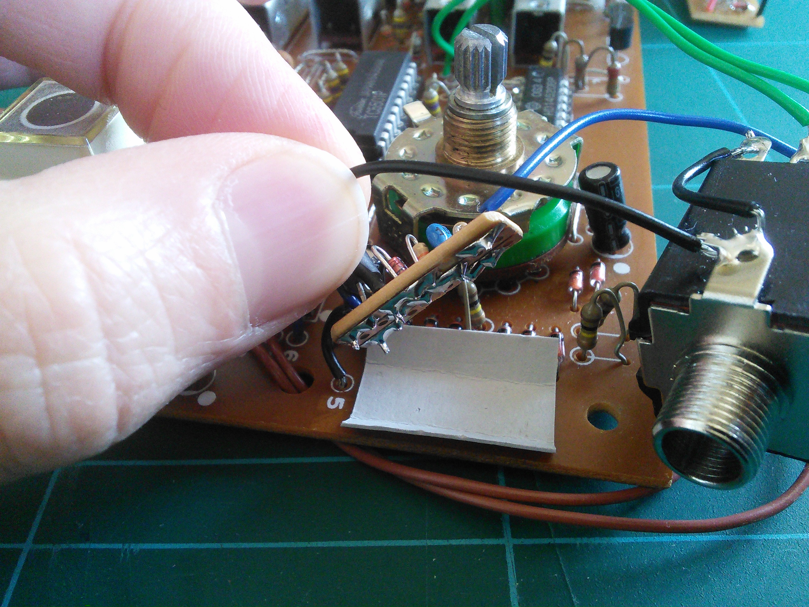
I built both these circuits onto a small piece of stripboard mounted onto the panel with one of the minijacks. There’s just enough room, as can be seen in the photos. This allows the use of both halves of a dual op-amp so nothing goes to waste. There’s also plenty of room on the experiment pads at the top of the Werkstatt’s PCB, though you may find it a bit cramped if you’ve already got a couple of mods in there like I have…
The photos show the locations on the PCB of the various supply rails you’ll be wiring up to: -9V and +9V to power the op-amp, +5V for the VCO amplifier reference, and GND. These are all labelled on the top side of the PCB anyway so it’s easy to find them. I shared the ground that my existing mods were already using, which is connected to the nearby screw post via a solder tag. See my CV mod for details.

Werkstatt VCO and VCF direct out mod wiring

Werkstatt VCO and VCF direct output mod installed

Werkstatt VCO and VCF direct output mod external appearance

Before and after: VCO and VCF direct outs. Top image 1V scale, bottom image 5V scale
Parts
U1: TL072 or equivalent
R1, R5: 10k (1/4W 1% Metal Film used here, but it’s not critical)
R2, 3, 6, 7: 20k
R4, 8: 1k
jacks, wire, stripboard: as per your own choice
Moog Werkstatt: adding a VCA CV input jack
I’ve already blogged about the reasons you might want to mod your Werkstatt, and have posted a list of mods here, so to complete the VCO/VCF/VCA trio, here’s the VCA input at last!
How it Works
This is a very simple mod, and just replicates the existing patch header input. All you need is a 10k resistor, some wire, and a jack socket.

Werkstatt VCA CV input mod schematic
The easiest point to solder to on the board is JMP62. This is located just above the Decay pot. This point is where incoming VCA CV signals are passively mixed. It’s probably best to solder the new parts to this jumper on the underside of the PCB, which you can see on the photos of the wiring:

Werkstatt VCA input: JMP62 location

Werkstatt VCA input: JMP62 on underside of PCB

Werkstatt VCA input: soldering

Werkstatt VCA input: side panel
Parts
10k resistor
Jack socket
Wire
Further thoughts
As the Werkstatt already has a pin for VCA modulation on its patch header, you might think this mod seems less immediately useful than the VCO or VCF CV inputs. The main issue is that there is no way to simply switch off the Werkstatt’s own VCA – you can select EG shaping, or ‘on’ for drones, but you can’t bypass it for use with an external envelope. What does this mean in practice, and why bother adding a CV input for it?
If you’re using the Werkstsatt with a modular, you’ll have more interesting envelopes than the attack-decay type on the Werkstatt. You might well also have something that will give an offset. It should be possible to use a negative offset to counteract the Werkstatt’s ‘on’ VCA CV, and mix in a more interesting envelope signal; setting the Werkstatt’s VCA to ‘on’ and feeding this CV input with that mix will then allow you to contour the Werkstatt’s VCA as you like.
It would also allow you to use the Werkstatt’s own patchbay to feed the VCA with its LFO, and simultaneously blend another LFO in with this CV mod. Mixing different LFOs gives a lot of movement to a sound, and can be very enjoyable to play with. You can also sequence the VCA level this way, while retaining other modulation via the pin header.
As always, my mods are not definitive – the best thing to do is experiment, and adapt, and find out what works for you and this excellent little synthesizer. Enjoy!
Envelope Circuits: a simple discrete AR design
As a companion to my simple op-amp AR envelope circuit, here’s a discrete version. It has the same basic functionality – gated input, variable attack and release times – but is made with transistors instead of integrated circuits. Power consumption is very low (just a handful of mA), and it runs from a positive supply of your own choosing. Like its op-amp cousin, it could be powered with a battery, or in a Eurorack system, or you could add it into an existing synth like the Moog Werkstatt as a mod.
The main difference between this and the op-amp circuit, aside from it being discrete, is that I have included a very simple way to set the level of the envelope output (see below for details).
RV1 is Release, RV2 is Attack. The Gate input can be anything over a couple of volts. Negative-going inputs (eg., from a bipolar LFO) will be removed by D1. The output goes to nominally 0V when fully off (closer than the op-amp version, in fact).

Discrete AR envelope schematic
Parts List
R1, R2, R6, R7, R10: 100k
R3, R4: 47k
R5, R8: 560 Ohm
R9: 24k
R11: 10k
R12: 1k
RV1, RV2: 1M linear pot
C1: 1µ non-polarized
D1, D2, D3: 1N4148 or equivalent
Q1, Q4, Q5: BC549C or equivalent
Q2, Q3: BC559C or equivalent
*
How it works
Compare the first pair of transistors with my discrete gate buffer circuit. A positive voltage on the input turns on Q1, taking the base of Q2 low. This turns on Q2, taking its collector high. This is how we drive our envelope.
Now compare the diode and potentiometer arrangement with my op-amp AR. Once you’re past the transistors, it works in basically the same way.
Q3 inverts the output of Q2, so when Q2 is on, Q3 is off, and vice versa. When the collector of Q2 is high, the capacitor charges through diode D3 and pot RV2 (Attack). When the gate input goes low, the transistors Q1-3 switch off, off, and on, respectively. In this state, the capacitor discharges through RV1 (Release) and D2.
Note the two 560 ohm resistors: one on the emitter of Q2, the other on the collector of Q3. When the gate input is high and the capacitor is charging, current flows through Q2’s emitter resistor; when the gate is off and the capacitor is discharging, current flows through Q3’s collector resistor. These two resistors put a lid on the current flow and limit the fastest times for Attack and Release. The value is a trade-off between current and snappiness. With the values shown, maximum current through these resistors is around 16mA and the fastest rise and fall times of the envelope are around 2ms.
The final two transistors in the circuit after the capacitor are the output buffer; notice the two resistors between them, forming a potential divider. With the values shown, if you run this circuit on 12V, the envelope output will be around 8V max.
There are better ways to set the peak level of an envelope, but my aim here is to keep things simple as a base for experiment.
Changes
The most obvious things to tweak are the envelope times and the output level.
The values of the two potentiometers affect the attack and release times, but the envelope can be substantially stretched by using a larger capacitor. It would be easy to add a switch that connected, say, a 4.7µF or 10µF capacitor in parallel with the existing one, which would multiply the envelope’s times substantially (use perhaps a 25V electrolytic, with its -ve terminal to ground).
The two resistors between the output buffer transistors can be adjusted to suit your requirements. If you want full-scale output (ie., envelope peak closer to the supply voltage), remove R9 and R10, and connect the emitter of Q4 directly to the base of Q5. In fact, this circuit will also work with just a single NPN as a buffer (miss out Q4 and the divider resistors, connect the cap to the base of Q5), but amongst other things the ‘zero’ value is less close to actual zero; if you want to experiment with a single transistor here, setting the level of the output can be done by replacing the 10k resistor on its emitter with a pair of resistors as a potential divider, or even a 10k trimmer with the output taken from the wiper.
Feel free to experiment with the circuit in Falstad’s handy online simulator.
Boss DR-55: external trigger input mod
By default, the Boss DR-55 does not receive any kind of incoming clock. The ‘FS’ footswitch input takes a latching footswitch that starts and stops the existing clock, but that’s it. Although you can clock other equipment from the DR-55, it would be nice to be able to use an external clock to sync the Boss to, which would allow the Boss to trigger yet more devices with its CSQ and DBS outputs (active on Accented steps only and every step, respectively).
My mod as detailed here does exactly that. By replacing the existing FS jack socket, adding a small circuit, and replacing a jumper, we can safely trigger the DR-55 from an external trigger.
A quick internet search will turn up an existing clock input mod which is simpler to do and requires no extra parts; however, it puts the RAM at risk of damage from high triggers, and it does not sync the Boss’ own DBS output. It also requires ‘arming’ by hitting start before external triggering.
My own mod, though more complex, overcomes all these issues: the trigger input is protected, both the Boss’ trigger outputs maintain their correct functions, and triggering occurs without ‘arming’. The only two functional disadvantages of my mod are that you must set the Boss’ tempo to Fast, and to reset the pattern when stopped mid-way you need to remove the trigger plug. I’m going to blog another small mod which will overcome the latter inconvenience [EDIT: No I’m not! I sold both my 55s, thereby halting this particular project].
The Clock Modification in detail
Below is a diagram which shows everything you need to know about building this mod. Below that is a parts list. Key to this is the replacement FS jack socket; it needs to be TRS (ie. a stereo jack), with single pole changeover switches on the tip and ring contacts. I used a Lumberg KLBPSS3 (datasheet here, Farnell UK stock page here).
The additional circuit can be made very small indeed (3 rows * 8 holes on stripboard), and there is plenty of room for it inside the DR-55, particularly towards the right-hand end. The photos below illustrate my own placement.
There is one jumper to be removed, the one immediately to the right of the Variation switch. The replacement connections for the upper and lower point of this removed jumper are shown in the diagram, and you can see in the photos how I wired this up.
In brief: remove that jumper, solder the two points to two jack pins; build the extra circuit, and solder that to the jack and to the main PCB; replicate two of the pre-existing connections from the jack to the PCB. That’s it. I also stuck a small folded piece of card to the PCB to stop the extra circuit from shorting against components.

Boss DR-55 clock input mod
The image above is a jpeg; click here for a PDF: Boss DR-55 clock input mod revised
Parts list:
1 * TRS 2-pole changeover jack socket – eg. Lumberg KLBPSS3
2 * 47k resistors – I used 1/8W for their smallness
1 * 10nF capacitor – I used a ceramic, again for smallness, but polyester film etc. would be usual
1 * 1N4148 signal diode or equivalent
1 * BC549C transistor or similar standard NPN
Here’s the modified DR-55 (also incorporating my DC supply mod):

clock modded DR-55 overview
And here’s a close-up of the clock mod:

clock modded DR-55 close up
Here are two angles to show the extra circuit more closely:

clock modded DR-55 circuit A
clock modded DR-55 circuit B
*
How to use your new trigger input
The new trigger input will accept any positive pulse over a couple of volts. It’s edge triggered, so the pulse can be any length over a couple of milliseconds. The operating principle is to use the DR-55’s existing clock, but to gate it on for a very short duration; normally when the clock is gated off again, the pattern resets, but the new jack socket enables us to disable that by breaking the reset connection when a jack is inserted.
As I mentioned earlier, the Tempo must be set to Fast (ie. all the way clockwise) for correct function. This is because the DR-55’s clock, once triggered, finishes its pulse cycle. If this is longer than the incoming trigger cycle, it will ignore the new trigger; if we set the speed dial to its fastest, we can clock the DR-55 at any rate up to its natural maximum.
The pattern will cycle round as usual, but if you stop mid-pattern, new triggers will continue where they left off. To reset the pattern at this stage, you need to unplug the trigger jack and hit Stop. This is not ideal, I know, and I will be making an amendment to correct this later [EDIT: project halted, see above. I have no current plans to do any further work on the DR-55].
For now though, this mod works fine, as shown in the (slightly rubbish) video below:
Boss DR-55: a 9V DC input modification
One of the drawbacks of the DR-55 as it comes unmodded is the power supply. In its original form, the DR-55 takes only batteries, and though this might be good for reducing cable clutter and having to find yet another wall-wart, it does mean you need to keep a regular stock of fresh AAs, and can guarantee that just when you want to use it, your DR-55’s batteries are too drained for the unit to function correctly.
Luckily, it is a relatively simple process to modify the DR-55 so that it takes a commonly-found 9V DC supply instead. I provide instructions for this below. It’s not the only way to do the job, but this is how I did it, and it works just fine. Modding the DR-55 in this way means it no longer accepts batteries, which means two things: 1) you will need access to a 9V adapter, and 2) pattern data will not be retained on power-off. Given that filling the memory of this humble machine can be done in less than five minutes, and I never use this outside my own home studio, I never found memory retention to be an issue. It would be possible to design a DC input that also catered for memory backup via battery, but I’m not going there.
There are two basic stages to this modification:
- Making a 9V DC input: the basic voltage supply circuit
- Installing the Mod: adapt some wire links on the output jack and PCB
Making a 9V DC input
Because the DR-55’s RAM can be killed by voltages higher than around 7V, we take a 9V input and regulate it down to between 5V and 6V. I chose to use a 5V regulator propped up with a diode to give around 5.6V, but you could also use a 6V regulator and omit D2. The input jack I used is a 3.5mm mono minijack of the kind often used for audio and CV interconnects, mainly because I had lots of them and the holes are easier to drill than the larger ones needed for a plastic-bodied insulated barrel connector. Use whatever type you prefer, but note the polarity of your incoming DC, and don’t connect the +ve to the case… with a tip-positive 3.5mm jack, the sleeve of the input jack is connected to the shell of the socket, so it makes sense for that to be the ground. Some barrel connectors do likewise.
Here’s the schematic:

Boss DR-55 DC input mod schematic
Here’s the final circuit built onto stripboard. It will be panel-mounted using the socket:

DR-55 DC input build
Installing the Mod
Now we have a simple DC input, we could just solder the +ve and Gnd outputs to the corresponding solder points on the main board – that is, where the battery clip attaches. Black is ground, red is positive. This works, but you still need to insert an audio cable to turn the DR-55 on. I chose to remove that ‘feature’, as there are no longer any batteries to protect from accidental drain. It’s a simple mod that just means a couple of wiring changes.
The diagram below shows the required re-wiring. The audio output socket is wired by default to both ground and audio signal, as well as having two pins wired to act as a switch when a jack is insterted. We want to retain the audio and ground connections, but not the switch. We remove those wires and instead bridge the corresponding points on the PCB.

DR-55 DC output jack and PCB mod
Here’s a photograph of the full mod (note the wiring):

DR-55 DC input wired and complete
I damaged a track while desoldering the battery wires, which is why the red wire goes to the un-numbered hole next to point 9. They’re directly connected, happily.
Below are some photos of the hole I drilled for mounting the new DC input, and the final appearance when mounted and labelled with cheap Dymo (should have gone with black… oh well):

DR-55 DC input enclosure drilling

DR-55 DC input socket and label
So there you have it. My humble DR-55 now works from a regular 9V DC wall-wart supply, and switches on whether or not its audio is connected. The hardest part is putting the DR-55 back together again…
*
